

What is intrinsic semiconductor , Valence Bond Theory and Energy Band Theory - Param Himalaya
What is intrinsic semiconductor? Give examples.
The semiconductor in which the current carriers (holes and electrons) are created due to thermal excitation only across the forbidden energy gap is called an intrinsic semiconductor
A pure semiconductor is called intrinsic semiconductor. It has thermally generated current carriers. Germanium and silicon are frequently used as intrinsic semiconductors.
Explanation of Behaviour of Intrinsic Semiconductors on the Basis of Valence-Bond Theory.
Structure of an intrinsic semiconductor. The three dimensional diamond like structure for Germanium or silicon or carbon is shown in figure.
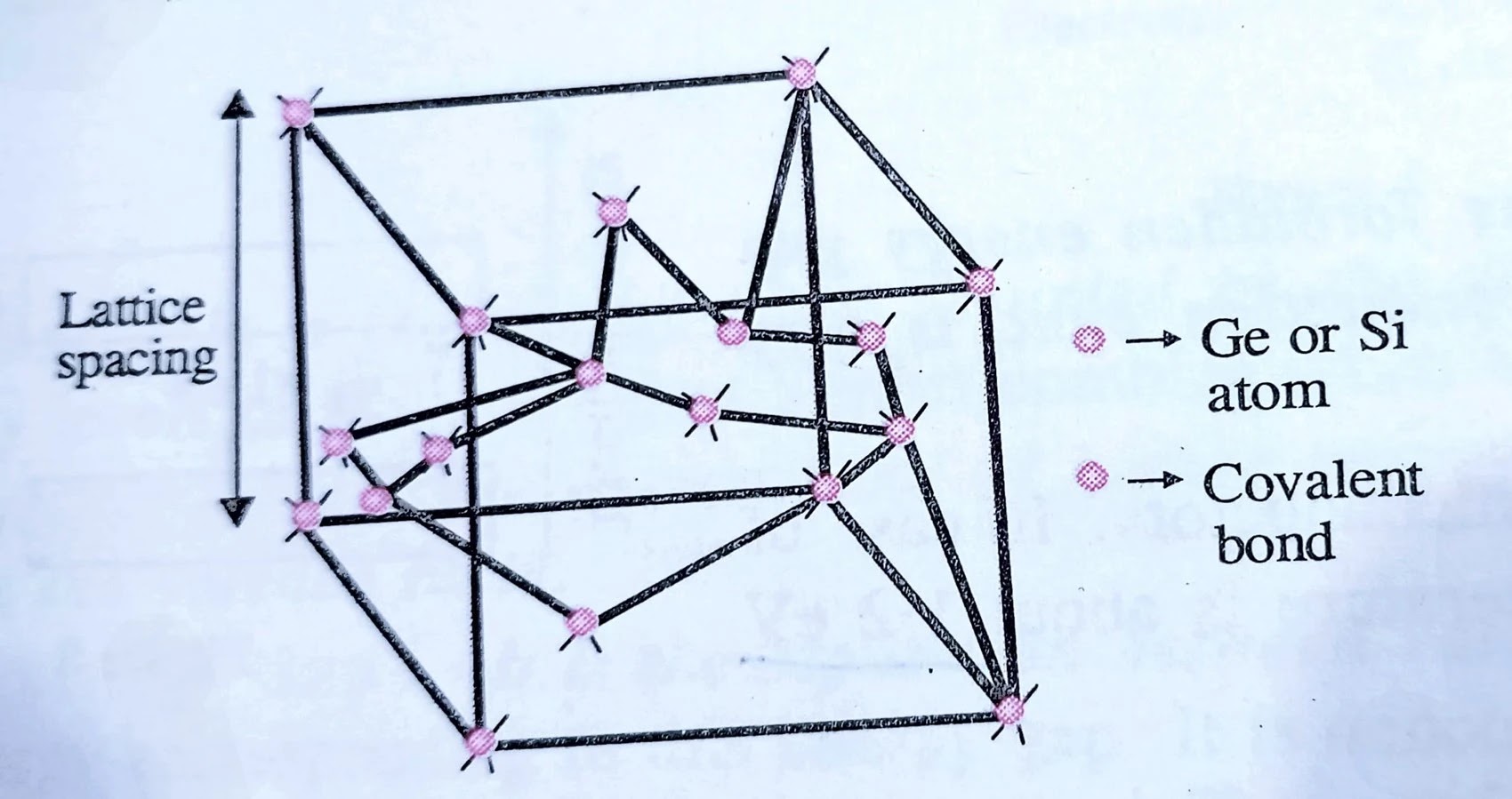
The lattice spacing for Germanium crystal is 5.66 A° the lattice spacing for silicon crystal is 5.43 A° and the lattice spacing for carbon crystal is 3.56 A°
Each atom of silicon (Si) and germanium (Ge) has four valence electrons (i.e., electrons in its outermost shell). In a crystal of silicon or germanium, each atom forms four covalent bonds (simply known as valence bond) by sharing its four valence electrons with the neighbouring four atoms.

At $0 \ \text{K}$ (very low temperature), all the covalent bonds are complete. Therefore, no free electron is available in the crystal for the conduction of current. Hence, silicon or germanium crystal behaves as an insulator at $0 \ \text{K}$.
Generation of electrons & holes. At room temperature, some of the covalent bonds will be broken because of the thermal energy supplied to the crystal. When a covalent bond breaks, an electron becomes free. The electron which leaves the bond is called free electron and the vacancy created in the covalent bond due to the release of the electron is called a hole (i.e., deficiency of an electron). The hole is equivalent to a positive charge ($+e$). This hole can be filled up by an electron from the neighbouring covalent bond, where another hole is created.

This process continues and the hole moves in the crystal lattice in random manner. In fact, movement of a hole represents movement of a bound electron.
Recombination of holes and electrons : Thermally generated electrons keep on occupying the positions of nearby holes. They collide with holes and recombine. This process goes on alongwith thermal generation of charge carriers (holes and electrons). At steady state equilibrium, rate of combination of holes and electrons is just equal to the rate of production of holes and electrons.
In an intrinsic semiconductor, the number density of free electrons $n_e$ (i.e., number of free electrons per unit volume) is equal to the number density of holes $n_h$ (i.e., number of holes per unit volume) is equal to the number density of holes $n_{h}$ and is known as number density of intrinsic carriers ($n_{i}$).
i.e.,
$$n_e = n_h = n_i ...(1)$$
where, $n_i$ is known as intrinsic carrier concentration.
Explanation of Behaviour of Intrinsic Semiconductors on the Basis of Energy Band Theory.
In a semiconductor, valence band and conduction band are separated by a forbidden energy gap $E_g \approx 1 \ \text{eV}$. The valence band is completely filled with electrons while conduction band is empty at $0 \ \text{K}$.

At room temperature ($T > 0 \ \text{K}$), the electrons in the valence band gain thermal energy and jump over the forbidden energy gap to reach the conduction band. The electrons reaching the conduction band leave behind equal number of holes in the valence band. These holes create empty energy levels in the valence band. The hole can be filled by an electron from the nearby energy level in the valence band. When the electron fills the hole, another hole is created at the site from where the electron goes to fill the hole.
Note :
- There are two kinds of current carriers in intrinsic semiconductors i.e., free electrons ($-e$) and holes ($+e$).
- The number of free electrons = number of holes in the intrinsic semiconductor.
- An intrinsic semiconductor is neutral as a whole.
- In a semiconductor, net current is due to the movement of both electrons and holes.
No comments:
Post a Comment